Friday, February 7, 2014

Retail Display/External Game Boy Displays


I found this really fascinating. In the video he says "we've added some really cool special electronics so that you can watch your game boy being played on a tv screen". I would love to know what electronics! Would it be difficult for someone today to build a gameboy to CRT converter? I couldn't find any schematics for the retail display.


You can see a ribbon cable going into the game boy itself, and a small electronics board - but I think it's just the volume controls. It's not at all clear how this device works!


A separate kiosk/external display was based on the NES, it uses a board called the Demo Vision (thanks to Retrogamer72 of nintendoage for the tip!):

from assembler games thread
For example, this was used inside this kiosk:
and here is a picture of the back of the modified () gameboy that you use it with:
It's not clear how the gameboy has been modified, maybe it's just an extra long ribbon cable soldered on?


To ease the strain on the eyes of developers working and testing a game, there was the wideboy:
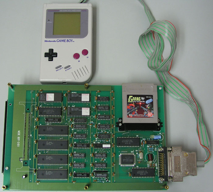
picture from the handheldmuseum
This plugs into a famicom/NES and lets you play game boy games on a screen - it's basically a NES cartridge with a gameboy CPU on it! Another page on the wideboy here.

A similar type of thing called the wideboy64 exists, letting you play game boy color games on an N64!

picture from chrismcovell.com/wideboy64
These were never available to buy (because they were either used in retail store displays or just for developers) but the GameBoy Booster was sold which let's you play game boy games on an n64:

picture from chrismcovell.com/gbbooster


A really cool hack someone did is interpreting the game boy signals from the ribbon cable using a microcontroller (but I have read that an FPGA is much more suitable) and then converting it into data for an oscilloscope to display:

See his blog here
And a video of it in action:


Another amazing hack, A gigantic LED matix being driven by a real gameboy through an FPGA:


Wednesday, January 22, 2014

Graphics: Tiles

All the graphics on the game boy are based on 8x8 tiles with 4 shades (2 bits per pixel), so 16 bytes each. The CPU uploads tile "character" data (pictures) to the video memory and then the background image (an optional overlay window) and sprites are all made by putting tiles together.

For an example let's look at the heart graphic from Super Mario Land:


It is stored using the following 16 bytes:

0000 6e6e bf93 bf83 ff83 7e46 3c2c 1818
 
translated to binary:

00000000
00000000

01101110
01101110

10111111
10010011

10111111
10010011

11111111
10010011

01000110
01111110

00111100
00101100

00011000
00011000

and the pixel shade is worked out using the following table:

0 white
0

1 light
0

0 dark
1

1 black
1

You can view the tiles inside a ROM image by converting every 16 bytes into image data this way, here are a couple of examples:


Boot ROMs

When you first turn on the game boy the Nintendo Logo will scroll down the screen and it chimes before the game starts, or if you don't have any game cartridge in it will show a black square like in this video:


What is happening when you first turn on the game boy is that it maps a "boot ROM" that's hard coded into the CPU over the memory range 0x0000-0x0100, it starts off by executing this program (which includes scrolling down the logo as well as initializing some CPU settings) before control flow is given over to the game cartridge itself.

A lot of specific information about the boot rom is described in Patent 5134391: System for preventing the use of an unauthorized external memory, but in particular at the very end of execution it maps the cartridge back over the range 0x0000-0x0100 so that a game can't read the boot ROM at all: That means you can't just create your own game cartridge that prints out the code inside the boot ROM.

In fact no one extracted the boot ROM from the game boy until neviksti in 2003 - 14 years after the Game Boy was released. This was done by decapping this chip and locating the part of the chip which actually encodes the boot ROM:

and then zooming in to it and reading off the individual bits by eye!


given that you can disassembly it from binary into assembly code that shows al the operations that the boot ROM does, you can read that commented here on the gbdev wiki and it really does follow the flow chart given on the patent almost by the letter:

The boot ROM for the game boy color was dumped in 2009 (almost a decade later) by a different technique using overclocking to skip that last instruction which locks out the boot ROM. You can read about that here: http://www.fpgb.org/?page_id=17.


The CPU

The CPU of the game boy handles almost everything except graphics, it does all the memory mapping and even sound synthesis. Here is a block diagram abstractly showing all the main components of the CPU:

Registers and Opcodes: The 8-bit registers come in pairs so that e.g. de and hl are often used as 16-bit numbers. There is a normal opcode table (with just a couple unused opcodes) and an extended opcode table for bit operations so just under 2x256 operations.

Memory Mapping: The CPU itself builds a memoy map that lets it address (using numbers from 0x0000 to 0xFFFF) various different chips like the two SRAM shown earlier as well as memory on the cartridge/game-pak inserted , there are also many specific addresses that act as hardware registers and this is how it interfaces with the serial port, lcd display, sound synthesis etc.

Interrupts: The CPU also supports interrupts via the interrupt controller. These  are triggered by special hardware events, during code execution the program-counter can jump to execute an interrupt routine to handle the event before returning back.

DMA: There is also a feature called Direct Memory Access which enables it to copy blocks of data around while executing other instructions.

Here are microscope photographs of one of these CPU chips decapped:

taken by Epop

and this fantastic image from tinytransistors (the link includes zooms of specific parts and descriptions of what they are)
Sources & Links:

Overview

Here are the main parts of the game boy unit:

The second block diagram (from patent 5134391) shows that the LCD controller is split into two parts.

and here is the main PCB from a real game boy:


You can see the main CPU in the middle, the two SRAM chips  used for display and work memory and I think the fourth chip amplifies the sound. At the bottom you can see where the cartridge (game pak) connector has been removed.

In the block diagram "6-pin subconnector" is the link cable port, here are pinouts for it and the cartridge connector


I think that the CPU itself outputs a stream of pixels which the two LCD chips (see the schematics) then decode into vertical and horizontal lines. You can see both those chips (covered in a glob) one behind the screen in this image, and the other on the flexible PCB below the screen:

Sources: